(理工学部、建築・環境学部教養学会主催ミニ講演会)
第71回理科系学生のための公開英語講演会
Miniaturization of Electric Devices:
The Latest Report from Germany
電子デバイスの小型化:ドイツよりの最新研究報告
講師: 理工学部理工学科 表面工学コース
小岩 一郎 先生
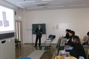
On December 2nd, 2024, a regular session of the English Lecture Meeting for Science Major Students was held under the sponsorship of the Academic Society of Faculty of Liberal Arts, inviting Dr. Ichiro Koiwa at the College of Science and Technology to give a lecture with the above title, which was the third opportunity on which the lecturer gave a talk to the audience consisting mainly of science major students.
In the introduction of this lecture, Dr. Koiwa talked about electronic devices in their early stages, mentioning specifically that in those days stereo amplifiers for audio equipment had many vacuum tubes and metal wirings; besides, one vacuum tube was 10 centimeters long. Naturally, at this stage of the development of electronic devices, no one had dreamed of having wearable equipment as we do today. The audience were surprised to find that the first computer in the world fabricated in 1946 had as many as 18 thousand vacuum tubes and weighed 27 tons.
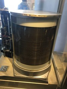
The lecturer went on to introduce the first disc drive that IBM developed in 1950s named RAMAC (the photo shown below), which was as large as a refrigerator, equipped with 50 sheets of 24-inch disc drives, and had a storage capacity of 5 megabytes. He emphasized that the most notable contributor to the current electronics industry was the development of “the integrated circuits.”
With the advent of modern electronic devices which by now we are familiar with, the period of vacuum tube was ended and came a new era of solid-state electronics with semiconductors or integrated circuits (IC).”
The lecturer mentioned how the semiconductor has developed since the beginning of its history in the early 20th century, especially how densely it has been integrated in a circuit, in reference to Moore’s law, a prediction made in 1965 by Gordon Moore, the co-founder of Intel that the number of transistors in an integrated circuit would double every year. Notably, the lecturer pointed out that currently, the increase in storage capacity of electronic devices is progressing faster than their miniaturization.
Dr. Koiwa also referred to an astonishing development in the latest optical lithography technology for manufacturing integrated circuits (ICs) known as EUV (Extreme Ultraviolet Lithography). So far, an outrageous amount of money has been invested in the development of this cutting-edge technology of lithography, so that only one piece of equipment of EUV currently costs as much as 20 billion yen. Considering also that just one semiconductor manufacturing line costs as much as 700~800 billion yen, it is only natural that merely a handful of companies, concretely Intel, Samson, and TSMC (Taiwan Semiconductor Manufacturing Company), should have afforded to buy the lines and their equipment. As yet there has not been a single EUV machine introduced to manufacturing lines in Japan. Recently, however, the following good news has been announced: the first EUV machine will be introduced to this country and is expected to start its operation in the near future.
In the main part of this lecture, Dr. Koiwa took up and discussed various interesting topics such as the toughest electronic device, social systems in Germany, and differences in linguistic expressions among the three languages, English, Japanese and German.
The following represents one of the discussions in the Q and A session:
Q. The question is discussed in the text when Moore’s Law will come to an end. My question, which probably is significantly related to that question, is what the size limit of semiconductors is.
A. While yours is quite a good question, it is very difficult to answer. The reason is that many people mistakenly regard Moore’s law as a statement about the minimum size of semiconductors. In fact, it is not about the size but about degrees of accumulated components in a chip; in other words, it is about the number of transistors that can be built in in a chip. Viewed in this light, the pace of the advancement that Gordon Moore predicted is expected to reach its limit before long. Don’t worry, though! For we have some great news for you: currently, we are seeing advances of new technology called chiplets, which I would like to talk about at the next opportunity. If this technology is fully established and introduced into the semiconductor industry, there could still be room for further minimizing the size of semiconductors (, though we may not be able to further accumulate components in a chip).

