理工学部/建築・環境学部教養学会主催ミニ講演会
第53回理科系学生のための公開英語講演会
English Lecture Meetings for Science Major Students
Miniaturization of Electric Devices:
The Latest Report from Germany
『電子デバイスの小型化:ドイツよりの最新研究報告』
講師:理工学部理工学科、表面工学コース
小岩 一郎
理工学部、建築・環境学部教養学会では2022年12月5日にエレクトロニクス実装工学、薄膜工学の研究者である小岩一郎先生を講師として招聘し、「第53回理科系学生のための公開英語講演会」を開催した。
長年民間の研究所での半導体機器の設計、開発に携わってこられた講師の経験から、電子デバイスの小型化にまつわる以下のような様々な話題についてお話をされた。
1) 真空管と電気ワイアを用いた初期の電子デバイス
2) 半導体集積回路とプリント配線板を備えた電子デバイス
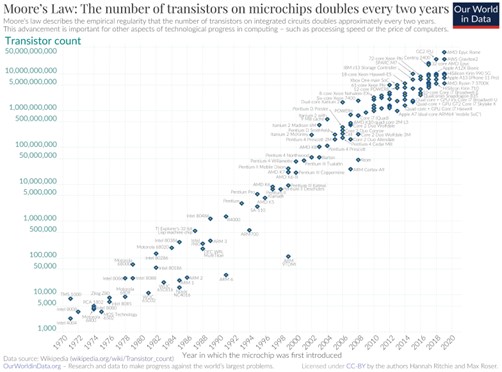
3) ムーアの法則とその変遷
4) ゲーム機における極小化
5) EUVリソグラフィ技術
6) 携帯電話における極小化
また、米国やドイツでの研究生活における経験談、ドイツ人と日本人との様々な日常生活の場面における行動や習慣の違い、あるいは専門用語のアメリカ英語の発音に関する注意なども行われ、両学部の理科系受講者の興味を喚起するとともに、理科系の研究者にとっての英語の運用能力の重要性が教示された。
受講者からは事後、本講演会において英語学習者としての学習動機づけが大いに高められた旨の報告が行われた。
小岩 一郎先生に感謝致します。
※画像はWikipediaより引用。
以下は当日の受講者よりの質問の一部。
Q. Professor Koiwa, do you think we will reach a limit to Moore’s Law sooner or later?
ムーアの法則には、いずれ限界は来るとお考えですか?
A. What a fantastic question! Currently, the size of the chips is becoming larger and larger due to the increase of their capacity. However, it is expected that as the size of the chip is enlarged, it will be difficult to produce as many chips as would fulfill the demand of the world market; besides, there would be produced a larger number of defective products whose size is also larger than that of the chips currently manufactured.
In order to resolve this problem, researchers have been trying to develop a new type of IC chip called “chiplet” for the last ten years or so. Instead of producing a larger-sized chip, they endeavor to produce a chip comprised of a few numbers of component chips with clearly distinct functions. Were this technology to be established in the future, Moore’s Law itself might finish its role in the history of the development of semiconductors. The idea of a chiplet could be a revolutionary development in this field. Let us keep paying attention to its development hereafter.
Finally, in connection with this issue, I should mention a problem with lithography: while the miniaturization of semiconductors requires technique to draw miniaturized electronic circuits, there is no established technique known for next-generation lithography. This is another important task which should go hand in hand with the development of chiplet in the near future.
Q. Before the public statement of Moore’s Law, what were the situations of miniaturization like? Was the electronics industry fervently pushing it forward?
ムーアの法則が公然と述べられる前は、小型化の状況はどのようなものであったのでしょうか?業界はそれを熱烈に推し進めていましたか?
A. When we characterize the nature of Moore’s Law, the most suitable word for its description seems to be “declaration of Gordon Moore’s hope (or his ambition, for that matter) for the future of Intel at the stage of 1965.” By announcing his future vision publicly, Moore attempted to lay down a new design rule of IC chips for the world industry to follow, thereby making a large profit for his own company. Therefore, as my answer to your question, I would like to suggest that your question should be better rephrased as “why, all of a sudden, has miniaturization been declared so loudly since 1965?”
2022年12月5日(月)開催